Attention
This documentation is a work in progress. Expect to see errors and unfinished things.
banyan_mem
Description
Single-buffered capture of raw ADC data
Hard-code number of ADCs at 8, at least for now
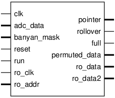
Pinout

Parameters
Name |
Min |
Max |
Default |
Description |
|---|---|---|---|---|
aw |
? |
? |
10 |
|
dw |
? |
? |
16 |
Ports
Signal |
Direction |
Description |
|---|---|---|
clk |
Input |
timespec 6.1 ns |
adc_data[8*dw-1:0] |
Input |
|
banyan_mask[7:0] |
Input |
must be valid in clk domain |
reset |
Input |
resets pointer and full |
run |
Input |
set to enable writes to memory; Modulate to take valid adc_data (See TB) |
pointer[aw+3-1:0] |
Output |
write location |
rollover |
Output |
|
full |
Output |
|
permuted_data[8*dw-1:0] |
Output |
|
ro_clk |
Input |
|
ro_addr[aw+3-1:0] |
Input |
|
ro_data[dw-1:0] |
Output |
|
ro_data2[dw-1:0] |
Output |
Implementation and use
The portable Verilog implementation can be found in banyan_mem Source File
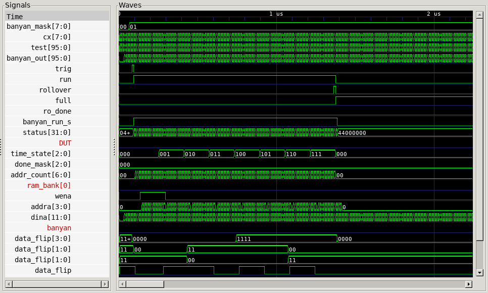
Timing Diagram
A GTKWave-generated timing diagram is shown below:
