Attention
This documentation is a work in progress. Expect to see errors and unfinished things.
dpram
Description
Dual port memory with independent clocks, port B is read-only
Altera and Xilinx synthesis tools successfully “find” this as block memory
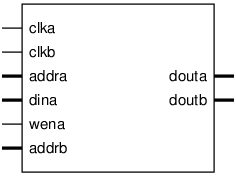
Pinout

Parameters
Name |
Min |
Max |
Default |
Description |
|---|---|---|---|---|
aw |
? |
? |
8 |
|
dw |
? |
? |
8 |
|
initial_file |
? |
? |
Ports
Signal |
Direction |
Description |
|---|---|---|
clka |
Input |
|
clkb |
Input |
|
addra[aw-1:0] |
Input |
|
douta[dw-1:0] |
Output |
|
dina[dw-1:0] |
Input |
|
wena |
Input |
|
addrb[aw-1:0] |
Input |
|
doutb[dw-1:0] |
Output |
Implementation and use
The portable Verilog implementation can be found in dpram Source File
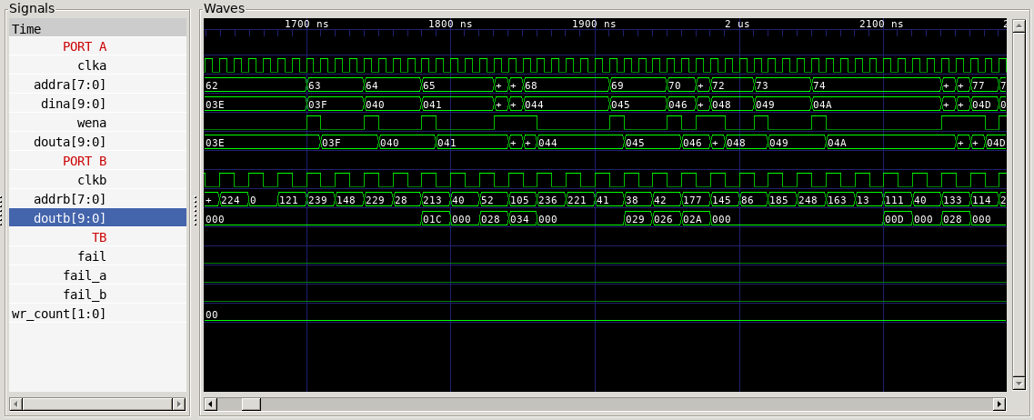
Timing Diagram
A GTKWave-generated timing diagram is shown below:
