Attention
This documentation is a work in progress. Expect to see errors and unfinished things.
complex_mul
Description
Complex number multiplication, as in
(a+ib)*(c+id) = (a*c-b*d)+i(a*d+b*c).
All the complex numbers are IQ-serialized, such that port x
carries a+ib, port y carries c+id, and port z carries the result.
It produces up to one answer every two clock cycles.
The 18-bit inputs and output are assumed scaled to [-1,1).
This module uses two 18-bit signed hardware multipliers,
and can clock at over 100 MHz in Spartan-6.
It’s pretty easy to ask for results that would overflow the representable
numbers; an extreme case is (1+i)*(1-i) = 2. All such results get
saturated to the maximum representable positive or negative number.
A second copy of the result with no rounding error is also provided
in z_all. Using both outputs will consume more FPGA resources than
using either one alone.
Output results are delayed four cycles from the input.
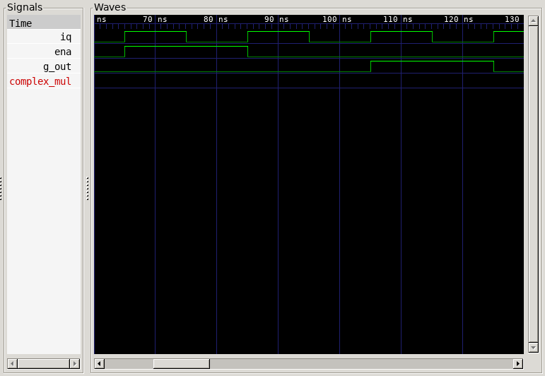
The gate_out port is nothing more or less than the gate_in
port, delayed four cycles. Only the iq control is used to control
the data paths inside this module.
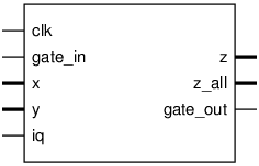
Pinout

Parameters
Name |
Min |
Max |
Default |
Description |
|---|---|---|---|---|
dw |
? |
? |
18 |
Ports
Signal |
Direction |
Description |
|---|---|---|
clk |
Input |
Rising edge clock input; all logic is synchronous in this domain |
gate_in |
Input |
Flag marking input data valid |
x[dw-1:0] |
Input |
Multiplicand, signed, time-interleaved real and imaginary |
y[dw-1:0] |
Input |
Multiplicand, signed, time-interleaved real and imaginary |
iq |
Input |
Flag marking the real (I) part of the complex pair |
z[dw-1:0] |
Output |
Result |
z_all[(2*dw)-1:0] |
Output |
Result |
gate_out |
Output |
Delayed version of gate_in |
Implementation and use
The portable Verilog implementation can be found in complex_mul Source File
Timing Diagram
A GTKWave-generated timing diagram is shown below:
