Attention
This documentation is a work in progress. Expect to see errors and unfinished things.
cpxmul_fullspeed
Description
————————————
cpxmul_fullspeed.v
Full data-rate pipelined complex multiplier with 3-cycle latency, 4 hw multipliers
and 2 adders
Expects time-aligned parallel inputs on all data inputs
————————————
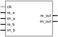
Pinout

Parameters
Name |
Min |
Max |
Default |
Description |
|---|---|---|---|---|
DWI |
? |
? |
18 |
|
OUT_SHIFT |
? |
? |
17 |
Down-shift full-precision result |
OWI |
? |
? |
18 |
Ports
Signal |
Direction |
Description |
|---|---|---|
clk |
Input |
|
re_a[DWI-1:0] |
Input |
|
im_a[DWI-1:0] |
Input |
|
re_b[DWI-1:0] |
Input |
|
im_b[DWI-1:0] |
Input |
|
re_out[OWI-1:0] |
Output |
|
im_out[OWI-1:0] |
Output |
Implementation and use
The portable Verilog implementation can be found in cpxmul_fullspeed Source File
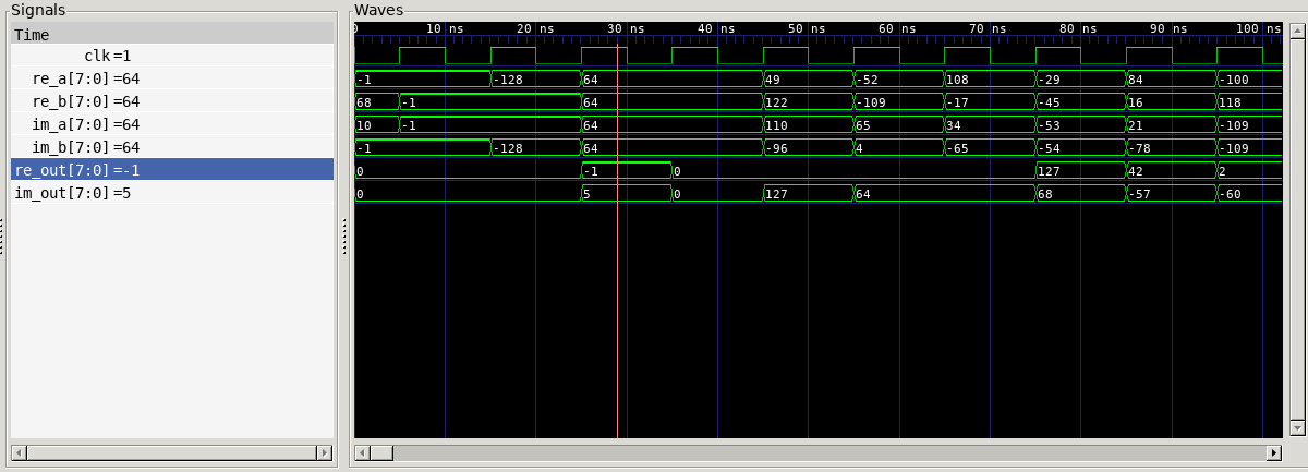
Timing Diagram
A GTKWave-generated timing diagram is shown below:
