Attention
This documentation is a work in progress. Expect to see errors and unfinished things.
lpass1
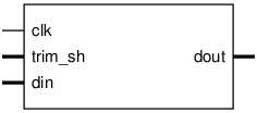
Pinout

Parameters
Name |
Min |
Max |
Default |
Description |
|---|---|---|---|---|
dwi |
? |
? |
16 |
|
klog2 |
? |
? |
21 |
Actual k is 0.5**klog2; max 31 |
TRIM_SHIFT |
? |
? |
2 |
Ports
Signal |
Direction |
Description |
|---|---|---|
clk |
Input |
|
trim_sh[TRIM_SHIFT-1:0] |
Input |
Move corner up in steps of 2x; Extra logic |
din[dwi-1:0] |
Input |
|
dout[dwi-1:0] |
Output |
Implementation and use
The portable Verilog implementation can be found in lpass1 Source File
Timing Diagram
A GTKWave-generated timing diagram is shown below:
