Attention
This documentation is a work in progress. Expect to see errors and unfinished things.
complex_freq
Description
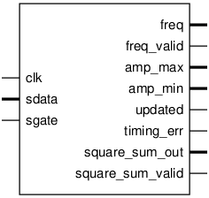
Pinout

Parameters
Name |
Min |
Max |
Default |
Description |
|---|---|---|---|---|
refcnt_w |
? |
? |
17 |
Ports
Signal |
Direction |
Description |
|---|---|---|
clk |
Input |
single clock domain |
sdata[17:0] |
Input |
|
sgate |
Input |
high for two cycles representing I and Q |
freq[refcnt_w-1:0] |
Output |
|
freq_valid |
Output |
Asserted when freq output is valid |
amp_max[16:0] |
Output |
|
amp_min[16:0] |
Output |
|
updated |
Output |
Asserted when amp_{max,min} are updated |
timing_err |
Output |
New data received while calculation is ongoing |
square_sum_out[23:0] |
Output |
|
square_sum_valid |
Output |
Implementation and use
The portable Verilog implementation can be found in complex_freq Source File
Timing Diagram
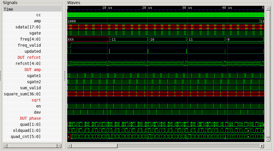
A GTKWave-generated timing diagram is shown below:
