Attention

This documentation is a work in progress. Expect to see errors and unfinished things.

rot_dds

Description

Phase Rotating Direct Digital Synthesis of sin/cos
18 bit output coming from cordicg
Note that phase_step_h and phase_step_l combined fit in a 32-bit word.
This is intentional, to allow atomic updates of the two controls
in 32-bit systems. Indeed, when modulo==0, those 32 bits can be considered

a simple fast binary DDS control for quirky (non-binary-rounding) phase
steps like:
7/33 for LCLS-II
8/11 for SSRF
9/13 for Argonne RIA

The phase generation algorithm
0. The phase increments for dds are generated using a technique described
in these 2 places:
Section: PROGRAMMABLE MODULUS MODE in:
Basically, increment the phase step at a coarse resolution, accumulate the
error on the side, and when that error accumulates to the lowest bit of
the coarse counter, add an extra 1 to the following phase step.
1. phase_step_h is the coarse (20 bit) integer truncated phase increment for
the cordic. There is a 1-bit increment of phase that comes from
accumulating residue phase.
2. This residue phase is accumulating in steps of phase_step_l, in a 12-bit
counter.
3. However, there will be an extra residue even for this 12-bit counter,
which is the modulus, and this added as an offset when the counter crosses 0

12-bit modulo supports largest known periodicity in a suggested LLRF system,
1427 for JLab. For more normal periodicities, use a multiple to get finer
granularity.
Note that the downloaded modulo control is the 2’s complement of the
mathematical modulus.
e.g., SSRF IF/F_s ratio 8/11, use
modulo = 4096 - 372*11 = 4
phase_step_h = 2^20*8/11 = 762600
phase_step_l = (2^20*8%11)*372 = 2976
e.g., Argonne RIA test IF/F_s ratio 9/13, use
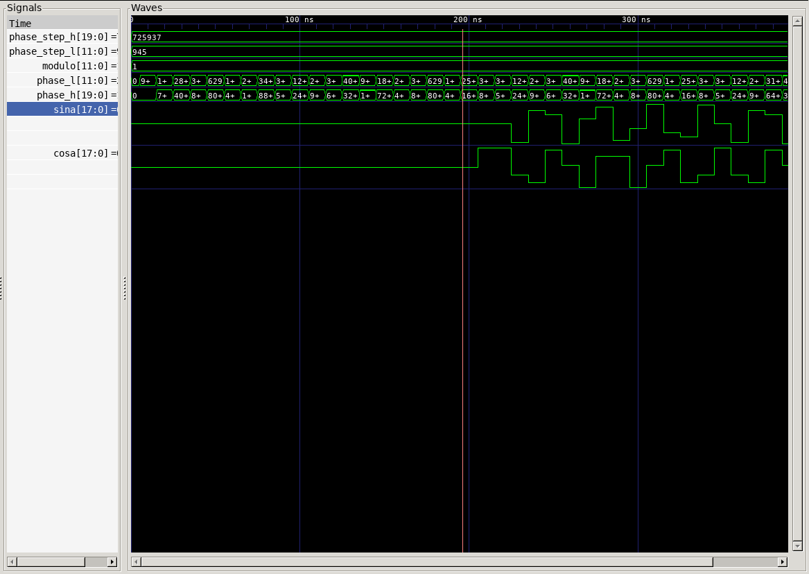
modulo = 4096 - 315*13 = 1
phase_step_h = 2^20*9/13 = 725937
phase_step_l = (2^20*9%13)*315 = 945

TODO:
Potentially, isolate phase generation into a separate module.
Haha, turns out there is ph_acc.v (We should USE it).
Synthesizes to ??? slices at ??? MHz in XC3Sxxx-4 using XST-??


Pinout
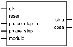
Schematic symbol

Parameters

Table 121 rot_dds_param_table

Name

Min

Max

Default

Description

lo_amp

?

?

18

Ports

Table 122 rot_dds_port_table

Signal

Direction

Description

clk

Input

timespec 9.0 ns

reset

Input

active high, synchronous with clk

sina[17:0]

Output

cosa[17:0]

Output

phase_step_h[19:0]

Input

phase_step_l[11:0]

Input

modulo[11:0]

Input

Implementation and use

The portable Verilog implementation can be found in rot_dds Source File

Timing Diagram

A GTKWave-generated timing diagram is shown below:
Timing diagram